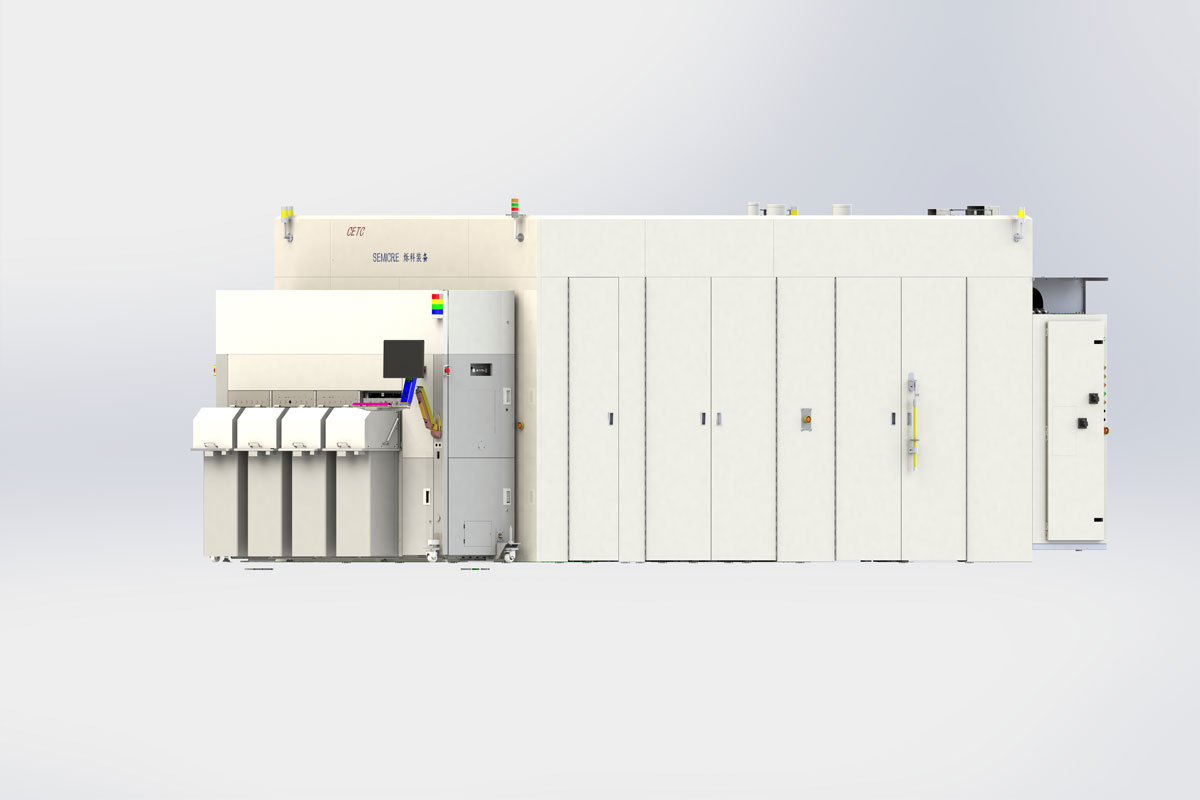
主要用途:用于SiC电力电子器件制造,Si基器件制造。通过向晶圆选择性注入掺杂元素如AI、B、N、P等,形成p-n结或调控器件性能参数。Main application: Focus on the manufacture of SiC power electronics devices and Si-based devices. By selectively implanting doped elements such as AI, B, N, P, As, p-n junctions can be formed and device performance parameters can be adjusted.
主要特点Main Characteristics:
1. 配置专用大束流Al离子源,维护周期大于300小时;Specified Al crucible ion source designed for high current applications, which makes PM intervals greater than 300h;
2. 适用于高温注入或常温注入,可配置高温加热靶或常温水冷靶,高温加热机械夹持靶台、高温静电吸盘、常温静电吸盘可选,最高加热温度超过600℃;Suitable for high-temperature or room-temperature implanting. It can be equipped with a high-temperature heating platen or a room-temperature water cooling platen. A high-temperature heating mechanical clamp, high-temperature E-chuck or room-temperature E-chuck is selective. The maximum heating temperature can exceed 600℃.
3. 配备束角度测量装置,注入角度控制精度高,束平行度优于0.2度;With a provided beam angle measure device, the implant angle is highly accurate, the parallelism is less than 0.2°.
4. 配置淋浴电子淋浴,降低晶圆表面静电积累;Using a selective PFG to reduce the electrostatics accumulation on the insulation layer of a wafer surface.
5. 可配置束流减速装置,最低注入能量低至5keV。With a selective beam decelerate devices, the minimum implant energy can reach 5KeV.
主要技术指标Main Parameters:
离子能量(Energy) | 5-200keV(单电荷Sinlge Charge) |
晶片尺寸(Wafer Size) | 4 inch/6 inch/8 inch |
剂量注入范围(Dose Range) | 2E11 - 1E16 ions/cm2 |
产品应用(Applications) | SiC, GaN等三代半导体器件制造(兼容Si基器件制造) Manufacture of the third generation of semiconductor devices(compatible with Si-based devices) |